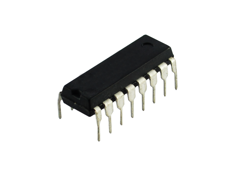
The HCC/HCF4032B and HCC/HCF4038B types
consist of three serial adder circuits with common
CLOCK and CARRY-RESET inputs. Each adder
has two provisions for two serial DATA INPUT signals
and an INVERT command signal. When the
command signal is a logical ”1”, the sum is complemented.
Data words enter the adder with the
least significant bit first ; the sign bit trails. The output
is the MOD 2sum of the input bits plus the carry from
the previous bit position. The carry is only added at
the positive-going clock transition for the
HCC/HCF4032B or at the negative-going clock for
the HCC/HCF4038B, thus, for spike-free operation
the input data transitions should occur as soon as
possible after the triggering edge. The CARRY is
reset to a logical ”0” at the end of each word by applying
a logical ”1” signal to a CARRY-RESET input
one-bit-position before the application of the first bit
of the next word.
